
X-ray Lithography in future Chip making
X-ray lithography works on a principle similar to other photolithography methods but with key differences
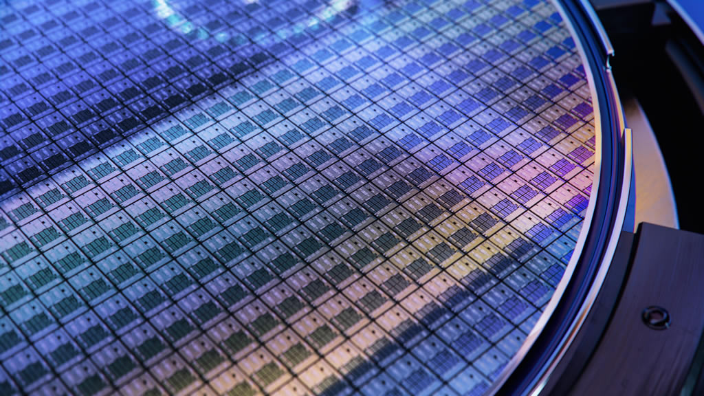
Process. A silicon wafer coated with a light-sensitive 'resist' is placed extremely close (within microns) to a patterned mask. Intense, collimated X-rays pass through the mask, exposing the resist in the pattern of the chip's circuitry.
Key Advantage. The extremely short wavelength of X-rays drastically reduces light diffraction, which is the fundamental physical limit to how small a feature can be printed with light. This allows it to achieve resolutions potentially down to the sub-nanometer range.
Core Challenge. At X-ray wavelengths, no material can effectively focus or refract the light like a glass lens can for visible light. Therefore, XRL must use 'proximity' or 1.1 printing, meaning the mask pattern is the same size as the final feature on the chip. This makes mask fabrication exceptionally difficult, as any defect or distortion is directly printed.
X-Ray future advantages and manufacture
Wavelength. 0.01 – 10 nm (Soft X-rays).
Resolution. Theoretically less than 5 nm, sub-nanometer.
Printing Method. Proximity 1.1 printing (no demagnification).
Light Source. Particle accelerators, synchrotrons, compact free electron lasers.
Primary Challenge. Mask fabrication, source power and size, resist chemistry.
R&D and prototyping. No commercial chip production.
Current EUV Lithography (e.g, ASML)
Wavelength. 13.5 nm.
Resolution. ~8 nm (single exposure, High-NA).
Printing Method. Projection optics (demagnifying mirrors).
Light Source. Laser pulsed tin plasma
Primary Challenge. Source power, optics complexity, cost.
High volume manufacturing for nodes down to 2nm (at present).
Current Research and Future Outlook
Startups Pursuing Integrated Systems. Companies like Substrate and Inversion Semiconductor aim to build entire new chip fabs around compact accelerator based X-ray sources. They claim a path to simpler patterning and a 10x cost reduction for advanced wafers by the end of the decade.
Academic Breakthroughs in Materials. Research teams, such as one at Johns Hopkins University are tackling the resist problem. They have developed new metal organic resists specifically tuned to absorb 6.x nm 'B-EUV' soft X-rays and enable high resolution patterning.
Path to Market. Most experts and companies involved see a 5-10 year timeline before the first production fabs could be operational. Its success depends on solving the mask and source challenges faster than EUV can evolve with techniques like Hyper-NA.
In summary, X-Ray lithography offers a compelling theoretical path to the smallest possible chips but faces a steep climb to overcome practical engineering and cost barriers that have stalled it for decades.